移至主內容

Technical Innovations at a Semiconductor Equipment Supplier in the AI Era

上午 11:35 - 下午 12:00

The AI era is both very exciting and very challenging; indeed, a semiconductor equipment manufacturer like Tokyo Electron must innovate aggressively to continue to enable the production of ever increasingly technically demanding device processing requirements.  This presentation will discuss some of the near future challenges for semiconductor processing, solutions for those challenges by Tokyo Electron, and how in this era, AI itself is being used to accelerate progress and the manufacturing challenges of the unprecedented build out of new semiconductor fabrication factories.


Key Technologies Covered

  • Industry market trends
  • Processing of very small 3D features
  • Advanced interconnect
  • Advanced bonding
  • Advanced patterning
  • The future of robotics and AI agents

Featured Speakers

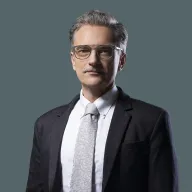
Dr. Peter Loewenhardt

Dr. Peter Loewenhardt

General Manager Technology Strategy, Tokyo Electron

Peter Loewenhardt is the General Manager, Technology Strategy, Customer Engagement Strategy Division at TEL presently living in Japan.  After joining TEL in February 2021, he has focused on semiconductor products technology and their respective roadmaps, matching them to the industry’s future requirements & needs.  Previous to TEL, Peter was at Applied Materials serving as Chief Technologist in Taiwan, and Field Technology in Europe.  He spent 13 years at Lam Research focusing on Etch and Wet Clean tool & process development and started his career at Applied Materials USA focusing on Etch and Dielectric CVD tool and process development.  Peter also researched fusion refueling at the California Institute of Technology and has a PhD in plasma physics from the Australian National University.

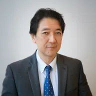
Dr. Akihisa Sekiguchi

Dr. Akihisa Sekiguchi

R&D Senior Vice President & GM, Tokyo Electron America

Dr. Akihisa (Aki) Sekiguchi currently serves as Senior VP & GM of Tokyo Electron`s US R&D Division.  Prior to this, he was Fellow of Tokyo Electron Limited`s Corporate Innovation Division.  Aki is responsible over 300 development engineers working in Albany New York, Austin Texas, and Fremont California, on advanced semiconductor process technology R&D.  He continues to be responsible for planning and executing worldwide alliance strategy for programs related to quantum computing application. 


He is currently on SEMI`s Board of Industry Leaders and is also a member of the CTO Forum representing TEL. 


In previous roles, he has led Corporate Marketing and Corporate Technology Development at TEL as the VP and GM.  


Prior to joining TEL in 2007, he worked for IBM Microelectronics Division for 17 years.  As part of Semiconductor Research and Development Center, he worked on the development of FEOL, MOL, and BEOL processes and equipment that enabled IBM`s DRAM and SOI based logic technologies.  During his last three years with IBM, he was responsible for process technology transfer from IBM to Sony (technology used in Play Station 3).


Aki earned his Ph.D. in Applied Physics from Columbia University, M. Eng. and B.S. in Engineering Physics from Cornell University, and an MBA in Finance from Stern School of Business (New York University, while working for IBM).  His doctoral thesis was on experimental plasma physics for thermonuclear fusion.