

Press Release: See Beyond the Surface: Accelerate Semiconductor Innovation with Advanced TEM Imaging and Analysis
As semiconductor devices continue to evolve toward sub-2 nm technology nodes, gate-all-around (GAA) transistors, 3D NAND, advanced memory, and heterogeneous integration, the demand for atomic-scale characterization has never been greater. Conventional inspection techniques can reveal surface features, but they often fall short when engineers need to understand buried interfaces, material composition, crystal defects, or process-induced variations that directly affect device performance and yield. Transmission Electron Microscopy (TEM) has become an indispensable technology for semiconductor development by providing the resolution and analytical capabilities needed to reveal the complete picture.
Thermo Fisher Scientific's advanced Transmission Electron Microscopy (TEM) and Scanning Transmission Electron Microscopy (STEM) solutions enable semiconductor manufacturers to visualize device structures with atomic-scale resolution while simultaneously performing comprehensive structural, chemical, and crystallographic analysis. These capabilities provide the "ground truth" needed to validate process development, optimize manufacturing, and accelerate failure analysis across logic, memory, power, and advanced packaging applications.
Atomic-Scale Insights for Next-Generation Devices
Modern semiconductor architectures incorporate increasingly complex three-dimensional structures with nanoscale features that require characterization beyond conventional microscopy. Advanced TEM imaging enables engineers to directly observe transistor gates, interconnects, dielectric layers, epitaxial structures, interfaces, and defects with sub-angstrom resolution. This level of detail is essential for understanding how structural variations influence electrical performance, reliability, and manufacturing yield.
Beyond high-resolution imaging, Thermo Fisher TEM platforms integrate multiple analytical techniques within a single workflow, allowing users to obtain comprehensive information from the same region of interest. These include:
- High-resolution TEM (HRTEM) and STEM imaging for atomic-scale structural analysis
- Energy-Dispersive X-ray Spectroscopy (EDS) for elemental composition mapping
- Electron Energy Loss Spectroscopy (EELS) for chemical bonding and compositional analysis
- Electron diffraction for crystal orientation, lattice characterization, and strain analysis
- Advanced imaging techniques such as integrated Differential Phase Contrast (iDPC), electron holography, Lorentz imaging, and electron tomography for specialized semiconductor applications.
Together, these complementary techniques allow engineers to correlate physical structure, material composition, crystallography, and electrical behavior, providing a comprehensive understanding of device performance.
Accelerating Process Development and Yield Learning
As semiconductor manufacturing becomes increasingly complex, rapid access to accurate characterization data is critical for shortening development cycles and improving production yields. Thermo Fisher's TEM workflow supports every stage of semiconductor innovation—from technology pathfinding and process optimization to root-cause analysis and production monitoring.
With automated imaging, high analytical throughput, and advanced software-assisted workflows, engineers can rapidly characterize process variations, validate new materials, investigate failure mechanisms, and perform statistically meaningful measurements with greater efficiency and consistency. These capabilities help manufacturers accelerate yield learning while reducing analysis time and operator dependence.
Complete Workflow from Sample to Solution
The quality of TEM analysis begins with high-quality sample preparation. Thermo Fisher delivers a complete semiconductor characterization workflow by integrating automated plasma focused ion beam (PFIB) and DualBeam™ systems with advanced TEM platforms. Site-specific sample preparation ensures precise targeting of nanoscale device features while minimizing preparation artifacts, enabling reliable and repeatable characterization results.
By combining automated sample preparation, high-resolution imaging, advanced spectroscopy, and intelligent software analytics, Thermo Fisher provides semiconductor manufacturers with a seamless end-to-end workflow that transforms complex device analysis into actionable process insights.
Enabling the Future of Semiconductor Manufacturing
Whether developing next-generation logic devices, optimizing high-bandwidth memory, improving power semiconductor reliability, or advancing heterogeneous integration technologies, TEM imaging and analysis provide the critical information needed to drive innovation with confidence.
Thermo Fisher Scientific continues to lead the semiconductor industry with comprehensive TEM solutions that deliver exceptional imaging performance, advanced analytical capabilities, and automated workflows designed to accelerate technology development, improve manufacturing yields, and enable the next generation of semiconductor breakthroughs.
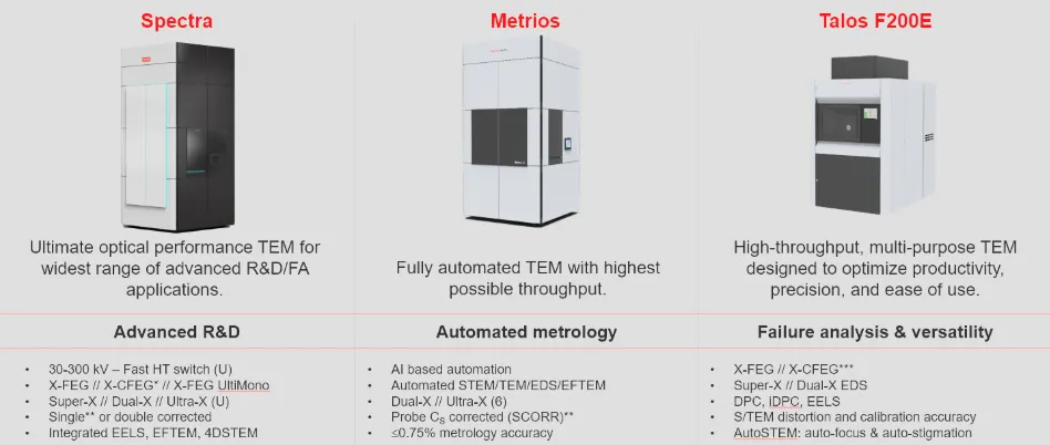
Figure 1. Thermo Scientific TEM portfolio for Semiconductor industry
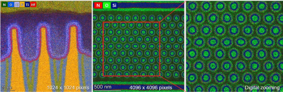
Figure 2. Thermo Scientific Talos F200E Dual-X EDS mapping on FinFET structure (Left) and 3D NAND (Middle and Right) samples.
About Thermo Fisher Scientific – Materials and Structural Analysis Division (MSD)
Materials and Structural Analysis Division (MSD), part of Thermo Fisher Scientific, is a global leader in analytical instrumentation and workflow solutions for the semiconductor industry, helping customers accelerate innovation from technology development through high-volume manufacturing. Through its comprehensive portfolio spanning Electrical Failure Analysis (EFA), Physical Failure Analysis (PFA), and Electrostatic Discharge (ESD) solutions, MSD delivers an integrated workflow that enables engineers to localize electrical faults, prepare precise samples, characterize complex device structures, and identify the root causes of device failures. By combining industry-leading technologies—including advanced electron microscopy, plasma and focused ion beam (FIB) systems, nanoprobing, automated metrology, and intelligent software analytics—MSD empowers customers to address the increasing complexity of advanced logic, memory, power, and heterogeneous integration devices. This end-to-end workflow helps accelerate root-cause analysis, improve yield, shorten development cycles, and enhance process control, enabling semiconductor manufacturers to solve today's most demanding technology and manufacturing challenges. As part of Thermo Fisher Scientific, MSD supports the company's mission to enable customers to make the world healthier, cleaner, and safer.