
Press Release: Accelerating Semiconductor Yield with the Thermo Scientific Helios MX1 PFIB-SEM
As semiconductor devices continue to evolve toward smaller geometries, more complex 3D architectures, and advanced packaging technologies, manufacturers face growing challenges in process control and yield improvement. Traditional inspection and metrology methods are increasingly limited when analyzing buried structures and subsurface defects. The Thermo Scientific Helios MX1 PFIB-SEM addresses these challenges by delivering automated, high-throughput 3D metrology and defect analysis directly at the wafer level.
The Helios MX1 PFIB-SEM is designed to accelerate time-to-data by combining plasma focused ion beam (PFIB) technology, ultra-high-resolution scanning electron microscopy (SEM), and advanced automation. Supporting both xenon and argon plasma ion sources, the platform enables optimized milling for different applications, ranging from rapid bulk material removal to precise cross-section preparation. Compared with conventional gallium FIB approaches, argon plasma milling significantly improves throughput for large-volume material removal while maintaining high-quality results.
Built for both fabrication facilities and analytical laboratories, the Helios MX1 features automated 300 mm wafer handling and fab host connectivity, enabling seamless integration into semiconductor manufacturing workflows. Engineers can inspect logic, memory, and advanced packaging devices with minimal manual intervention, helping shorten process development cycles and improve production efficiency.
One of the instrument's most significant innovations is its fully automated 3D reconstruction workflow. Following sequential milling and imaging, the software reconstructs complete 3D device volumes that reveal buried interfaces, hidden defects, and structural variations. Virtual slice metrology further enables engineers to examine critical dimensions from any orientation without additional destructive sectioning, providing richer process insights while reducing analysis time.
The Helios MX1 also introduces enhanced metrology software that streamlines recipe creation and automated measurement. Combined with high-performance computing resources, automated navigation, image acquisition, metrology, and reporting allow semiconductor manufacturers to rapidly identify process excursions and make confident decisions supported by statistically meaningful data.
Beyond speed, reliability is another major advantage. In-chamber calibration standards, automated performance monitoring, and standardized metrology validation help maintain measurement consistency across production environments. These capabilities reduce downtime while improving confidence in measurement repeatability.
As demand grows for AI processors, high-bandwidth memory, automotive electronics, and advanced logic devices, semiconductor manufacturers require analytical tools capable of keeping pace with increasingly complex device structures. The Helios MX1 PFIB-SEM enables engineers to 'see the unseen' by providing fast access to buried structures previously requiring laboratory-based analysis. Faster insights translate directly into accelerated yield learning, shorter development cycles, and improved manufacturing productivity.
With its combination of multi-ion PFIB technology, high-resolution SEM imaging, automated 3D metrology, and fab-ready integration, the Thermo Scientific Helios MX1 PFIB-SEM represents an important advancement in semiconductor process characterization. It empowers manufacturers to improve process control, reduce time-to-data, and confidently address the challenges of next-generation semiconductor manufacturing.
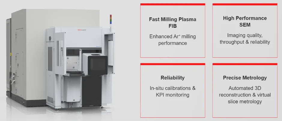
Figure 1. Thermo Scientific Helios MX1 Wafer-based PFIB-SEM tool and its strengths
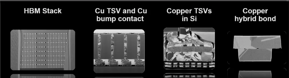
Figure 2. Thermo Scientific Helios MX1 Wafer-based PFIB-SEM application cases in Advanced Packaging device
About Thermo Fisher Scientific – Materials and Structural Analysis Division (MSD)
Materials and Structural Analysis Division (MSD), part of Thermo Fisher Scientific, is a global leader in analytical instrumentation and workflow solutions for the semiconductor industry, helping customers accelerate innovation from technology development through high-volume manufacturing. Through its comprehensive portfolio spanning Electrical Failure Analysis (EFA), Physical Failure Analysis (PFA), and Electrostatic Discharge (ESD) solutions, MSD delivers an integrated workflow that enables engineers to localize electrical faults, prepare precise samples, characterize complex device structures, and identify the root causes of device failures. By combining industry-leading technologies—including advanced electron microscopy, plasma and focused ion beam (FIB) systems, nanoprobing, automated metrology, and intelligent software analytics—MSD empowers customers to address the increasing complexity of advanced logic, memory, power, and heterogeneous integration devices. This end-to-end workflow helps accelerate root-cause analysis, improve yield, shorten development cycles, and enhance process control, enabling semiconductor manufacturers to solve today's most demanding technology and manufacturing challenges. As part of Thermo Fisher Scientific, MSD supports the company's mission to enable customers to make the world healthier, cleaner, and safer.