
VISION IV Corporation
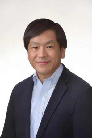 MR. Chiaki Ozeki, CEO, VISION IV Corporation
Chiaki was born in Yokohama, Kanagawa Prefecture. During his second year of high school, he studied abroad at United World College of the Atlantic in the UK. After earning a Bachelor of Laws from Kyoto University, he obtained a Master of Business Administration (MBA) from the Wharton School of the University of Pennsylvania. Following a 16-year career at foreign investment banks (Salomon Brothers, Goldman Sachs, and UBS), he held leadership roles overseeing M&A and finance at GE Japan and Nidec Corporation, and served as General Manager of the Corporate Finance Planning Department at Nikon Corporation. In 2021, he founded VISION IV Inc.
Topic:
Diamond substrates enabling next‑generation quantum sensing and extreme‑environment semiconductors.
Abstract:
VISION IV develops high-quality, scalable single-crystal diamond materials for semiconductor, sensor, and quantum applications. Our goal is to make diamond a critical industrial platform for next-generation electronics.
Silicon is reaching its performance limits, particularly under high temperatures, high voltages, radiation, and other harsh operating conditions. Diamond offers exceptional thermal conductivity, durability, energy efficiency, and the potential for highly sensitive sensing. However, commercialization has been constrained by difficulties in achieving the required wafer size, purity, doping control, and production scalability.
VISION IV addresses these challenges through an integrated platform combining CVD crystal growth, boron and nitrogen doping, stacking technology, quality engineering using the Taguchi Method, and in-house CVD equipment design. Our diamond materials range from 3 to 10 millimeters in size, reach thicknesses of up to 1.8 millimeters, and support boron concentrations from 10¹⁷ to 10²¹ atoms per cubic centimeter.
We apply this common technology platform across diamond electrodes, radiation and quantum sensors, and future power semiconductors. Target applications include aerospace, nuclear power, medical dosimetry, industrial detection, navigation, power infrastructure, and data centers.
We are seeking industrial development partners and preparing a US$10 million Series A round to expand equipment, working capital, engineering talent, business development, and overseas operations. Together, we aim to build the diamond-material foundation for a more efficient, resilient, and intelligent future.
Key Technologies Covered:
- Quality Engineering (Taguchi Method)
- Doping technology (Boron, Nitrogen)- highest concentration level of doing technology (patent filed)
- Stacking technology (resilient structure)
- Design capability of its own CVD equipment
- Handful diamond suppliers – need of SCM