
SandBox Semiconductor Incorporated
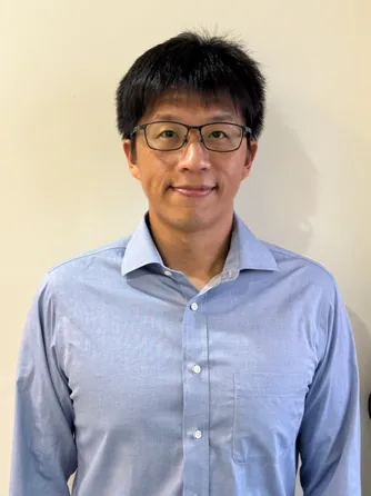 Mr. Yu De Chen, Application Manager, SandBox Semiconductor Incorporated
Yu De Chen is an Application Manager at SandBox Semiconductor, where he supports the adoption of AI-driven software solutions for semiconductor technology development. His work focuses on collaborating with customers to enable advanced process modeling, simulation, and data-driven engineering workflows for next-generation semiconductor applications.
With over 15 years of experience in the semiconductor industry, Yu De has held technical and engineering roles at Applied Materials, Lam Research, UMC, and TSMC. Throughout his career, he has focused on applying EDA and simulation technologies to address semiconductor process challenges, accelerate technology development, and improve engineering efficiency across advanced semiconductor applications. He has collaborated with global semiconductor teams to bridge process development challenges with software-based modeling and optimization solutions.
His professional interests include physics-based AI, EDA, process simulation, and digital engineering, with a focus on leveraging advanced modeling and intelligent software solutions to accelerate semiconductor technology innovation.
Topic:
Operational AI for Semiconductor Process Development
Abstract:
As semiconductor devices continue to scale, process development is becoming increasingly difficult due to growing complexity, longer development cycles, and an explosion of manufacturing data. SandBox Semiconductor helps customers transition from trial-and-error experimentation to predictive, model-based engineering. Our Physics AI platform combines first-principles physics, artificial intelligence, and automated metrology to predict process behavior, optimize recipes, and accelerate technology development before costly wafer experiments. Beyond building predictive models, SandBox helps customers deploy Physics AI within engineering workflows, making process expertise more scalable and accelerating engineering decisions across semiconductor R&D.
Key Technologies Covered:
• Physics-Based Artificial Intelligence (Physics AI) for Semiconductor Engineering
• Predictive Process Modeling and Virtual Process Development
• AI-Driven Recipe Optimization and Process Exploration
• AI-Enabled Automated SEM/TEM Metrology and Image Analysis