
AlixLabs AB
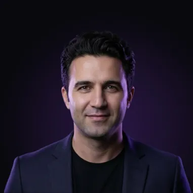
Dr. Amin Karimi, CTO, AlixLabs AB
Amin Karimi holds a PhD in Applied Physics from Lund University and joined the founding team of AlixLabs in 2020. His work focuses on establishing new patterning technologies for advanced-node electronics, and he has authored several publications and patents in nanotechnology. He is currently the CTO of AlixLabs, a Swedish semiconductor equipment company pioneering an advanced patterning technology called APS. In this role, he leads the development and industrialization of the company’s technology, working closely with engineers, research partners, suppliers, and customers to bring innovative semiconductor manufacturing solutions to market.
Topic:
Atomic Layer Etch Pitch Splitting (APS™): Cost-Effective Patterning for Advanced Semiconductor Nodes
Abstract:
Dense silicon line patterning is essential for advanced logic and memory devices, including FinFETs, gate-all-around transistors, gate electrodes, and metal interconnects. As semiconductor dimensions continue to shrink, conventional lithography and multipatterning techniques face increasing challenges related to resolution, cost, process complexity, defectivity, and pattern stability. This work presents Atomic Layer Etch Pitch Splitting (APS™), a patterning technology developed by AlixLabs that uses atomic layer etching to produce dense nanoscale features while extending the capabilities of conventional lithography. APS™ reduces pitch in a simplified processing step, decreasing the need for repeated deposition, lithography, cleaning, etching, and intermediate metrology. The technology supports patterns with different orientations and topologies and can be applied repeatedly for further pitch reduction. Using APS™, dense silicon line arrays with critical dimensions of 10 nm and a half-pitch of 10 nm were demonstrated. The approach offers a potentially more cost-effective, scalable, and sustainable alternative for advanced semiconductor patterning.
Key Technologies Covered:
- Semiconductor equipment manufacturing
- Advanced-node semiconductor fabrication
- Sub-2 nm technology-node patterning
- Nanofabrication and nanoscale process integration
- Atomic Layer Etching (ALE)
- Atomic Layer Etch Pitch Splitting (APS™)
- Cost-effective high-resolution patterning
- Lithography resolution enhancement
- Dense silicon line and feature fabrication
- Advanced logic and memory device manufacturing