Integrated Photonics: Innovations and Challenges in The Netherlands

3:50 pm - 4:15 pm

Within Europe, the Netherlands is one of the key hubs in integrated photonics. It has a thriving ecosystem around its core competencies in InP and low loss SiN platforms and packaging. Next to scaling pure play foundries in InP and SiN photonic chips, and the deployment of these chips in datacentres, new applications such as wireless optical communication, biosensors and others are emerging. Many PIC applications require a combination of platforms and integration with electronic chips. New technologies such as glass interposers and laser die transfer are being developed to enable this in mass production. 


Key Technologies Covered

  • Integrated photonics

Featured Speakers

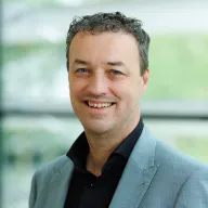
Dr. Ton Van Mol

Dr. Ton Van Mol

Managing Director PITC and TNO/Holst Centre, Photonic Integration Technology Centre

Ton van Mol graduated with honors from Eindhoven University of Technology in Chemical Technology in 1997, and received his PhD in the area of Thin film technology in 2001. He worked at Sandia National Laboratories (Livermore) as visiting scientist and joined TNO in 2003. In 2005, Ton helped set-up the open innovation initiative between IMEC and TNO called Holst Centre, where he became managing director in January 2015. In his role as MD of Holst Centre, Ton helped setup 10 spin off companies and helped grow Holst Centre from 75 to 130 R&D specialists in 2026.

In 2022, Ton initiated and is currently also managing director of PITC, the photonic integration technology centre, a strategic collaboration between TNO/Holst Centre, University of Technology Eindhoven, University of Twente, and PhotonDelta. PITC aims to help industrial companies in their development goals for integrated photonics technology through shared research programs. In 2025, the PITC partners became part of PIXEurope, the EU pilot line initiative, and Ton is leading the efforts of setting up a pilot line for 6 inch InP photonic chips with a capacity of 10.000 wafers/year.