Seiki Semiconductor Launches Dual-Mode Hybrid Bonding System at SEMICON Taiwan 2025.
New 82CWW Series enhances advanced packaging with precision, throughput, and Taiwan-localized manufacturing.
Taipei, Taiwan – September, 2025 – Seiki Semiconductor Co., Ltd. (Seiki Semi), a Japan-founded semiconductor equipment company, today announced the launch of its 82CWW Series dual-mode hybrid bonding equipment at SEMICON Taiwan 2025. This milestone underscores Seiki Semi’s commitment to driving innovation and advancing localized equipment manufacturing for Taiwan’s semiconductor industry.
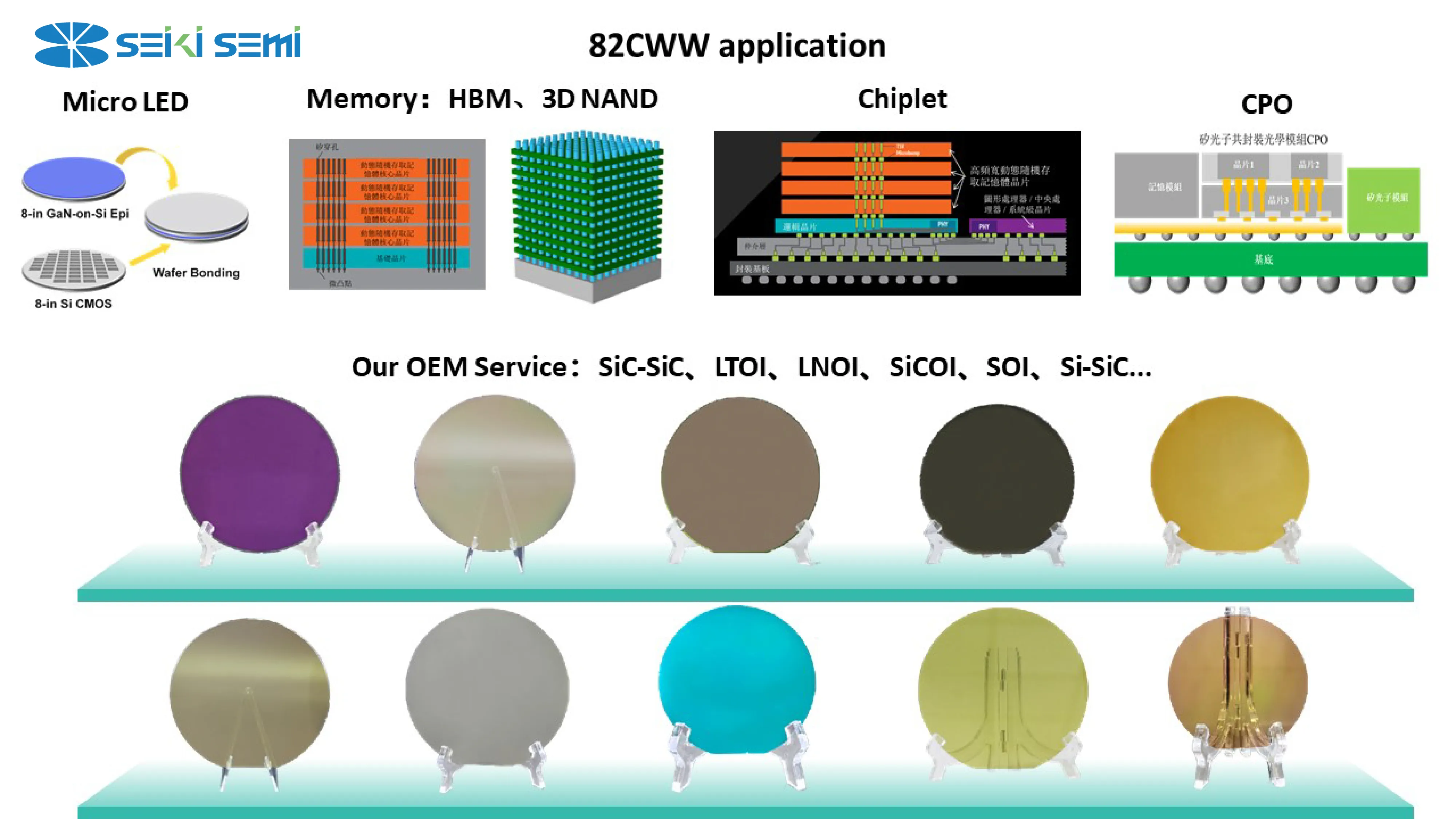
The 82CWW system supports both chip-to-wafer (C2W) and wafer-to-wafer (W2W) hybrid bonding, offering a scalable solution for R&D and high-volume production. Designed to meet the demands of advanced packaging, the system is compatible with 8-inch and 12-inch wafers and can handle ultra-thin wafers down to 35μm. It supports chip sizes ranging from 0.5×0.5mm to 50×50mm and achieves bonding accuracy of ±100nm with throughput up to 1,000 chips per hour.
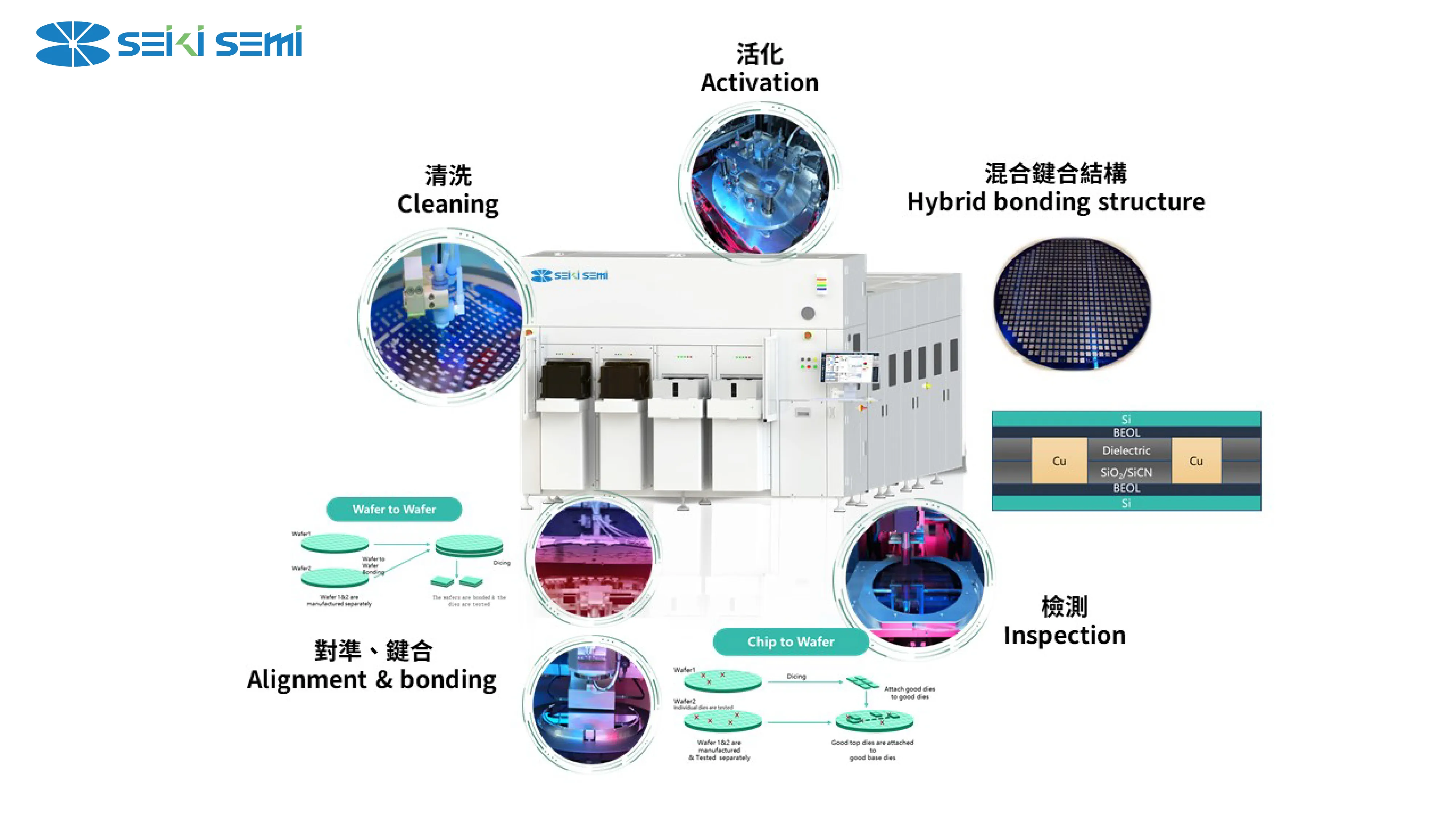
Key features include dual alignment methods (coaxial and infrared), modular part-swapping for rapid reconfiguration, and real-time offset compensation via integrated high-speed detection and feedback algorithms - all designed to maximize bonding precision, reduce downtime, and ensure consistent yield in both R&D and production environments.
As part of the SEMICON Taiwan program on September 9, Seiki Semi will also host a featured session by Professor Tadatomo Suga of the University of Tokyo, a pioneer in hybrid bonding technologies, who will deliver speech titled “Advanced Hybrid Bonding Technologies and Applications”, featuring how advanced packaging and 3D integration are helping overcome key system bottlenecks in AI and HPC, and highlight the need for cross-sector collaboration to drive continued innovation.
Hybrid bonding is rapidly emerging as a cornerstone technology in heterogeneous integration and 3D stacking, particularly amid rising demand from AI, high-performance computing, and automotive sectors. Seiki Semi is strengthening its commitment to R&D in Taiwan to support this evolution, reinforcing the region’s strategic role in the global semiconductor supply chain.
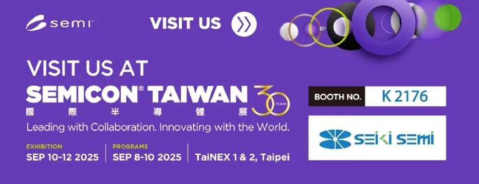
Visit Seiki Semiconductor at SEMICON Taiwan 2025 – Booth #K2176, floor 1, Hall 1
About Seiki Semiconductor
Founded in Japan and based in Taiwan, Seiki Semiconductor Co., Ltd. has over 20 years of experience in developing hybrid bonding equipment and processes for advanced packaging. Its technologies are applied to memory chips, CMOS image sensors, micro-LED displays, silicon photonics, and wafer-level heterogeneous integration. The company also provides OEM bonding services for semiconductor manufacturing.
Media Contact:
Seiki Semiconductor Co., Ltd. 青輝半導體股份有限公司
Jurgen Yeh葉國光
General Manager
[email protected] /+886 35973325 #3382/MP +886 922260881
www.seikesemi.com