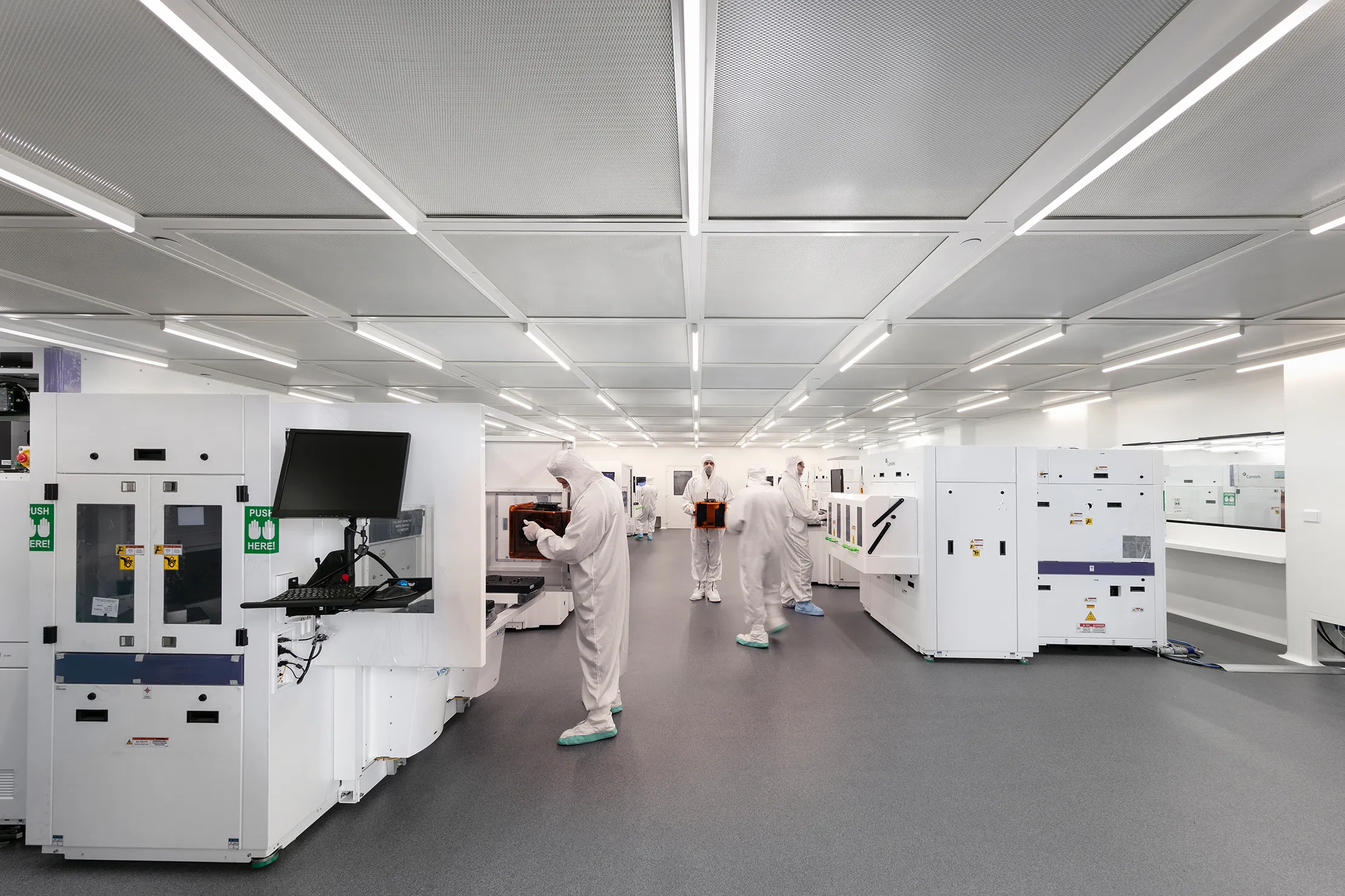
Camtek, a global leader in high-end inspection and metrology equipment for the semiconductor industry, will present its latest advancements in inspection and metrology technologies at SEMICON Taiwan 2025. Designed to support the semiconductor industry’s transition towards chiplet architectures, High Bandwidth Memory (HBM), and hybrid bonding, Camtek’s solutions empower manufacturers to achieve superior yield and process control across R&D and high-volume production.
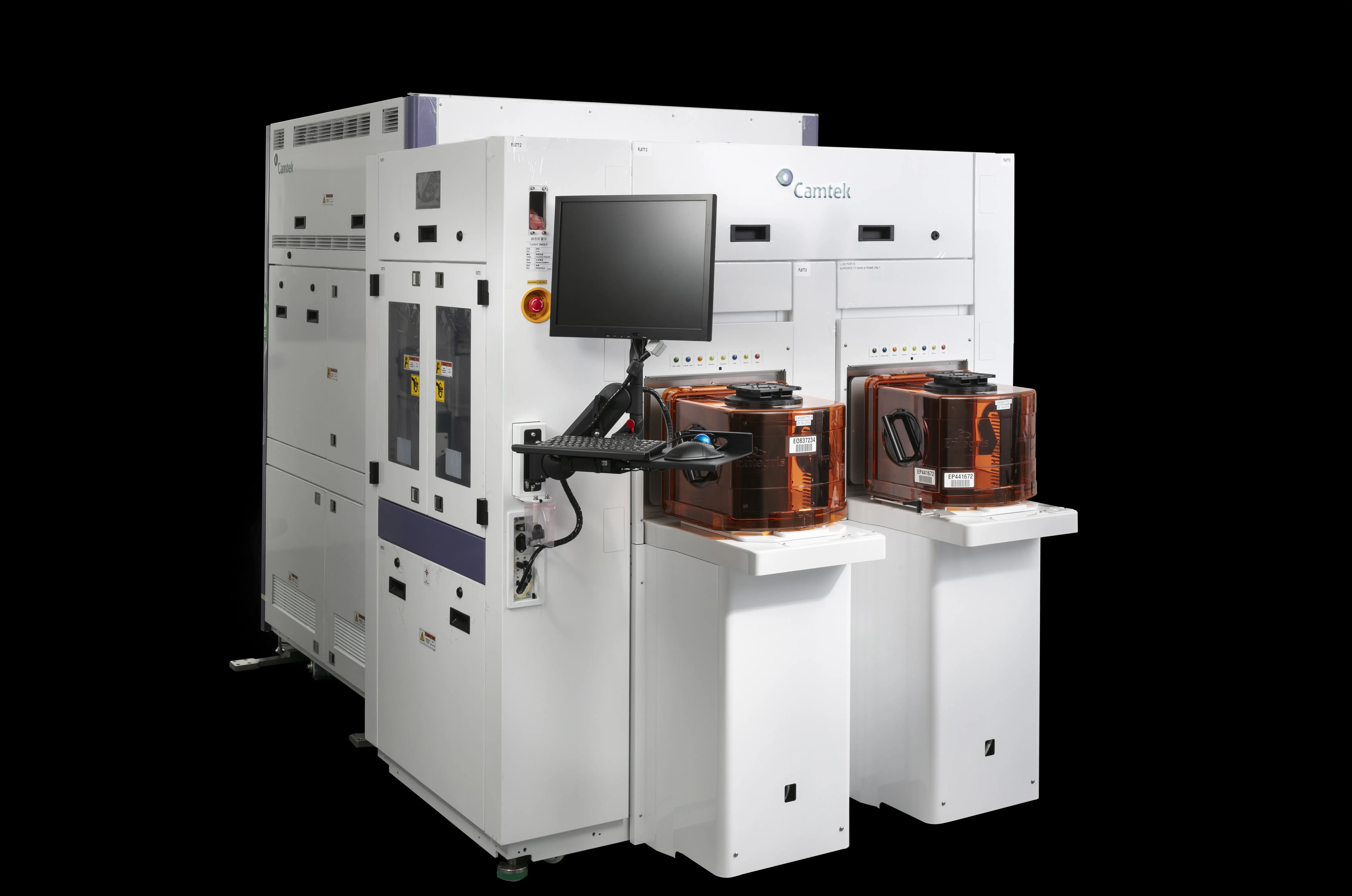
Camtek’s portfolio includes its Hawk product family, introduced earlier this year, which has been widely adopted for cutting edge advanced packaging applications: Chiplets, HBM and Hybrid Bonding. Camtek’s MicroProf product series offers advanced metrology capabilities, including Total Thickness Variation (TTV), wafer warp measurement, Through-Silicon Via (TSV) metrology, and overlay measurements for Redistribution Layers (RDL). These capabilities address the stringent requirements of next-generation devices, enabling manufacturers to maintain quality while accelerating time to market.
As the semiconductor landscape advances towards more complex packaging technologies, Camtek’s innovative solutions remain integral to ensuring defect-free products, faster ramp-up, and reduced time to market.
Visit Camtek Booth M1040 to learn how Camtek’s cutting-edge inspection and metrology solutions can help you stay ahead in the competitive semiconductor market.
At SEMICON Taiwan, Heterogenous Integration Global Summit, Camtek will present on the following topic:
Metrology Solutions in Advanced Packaging for 2025 and beyond, Mr. Alejandro Avellán, Heterogeneous Integration Global Summit 2025 – Day 2 on 11th Sep.
As we progress beyond 2025, the semiconductor packaging industry is set to undergo transformative growth, driven by advancements in artificial intelligence, automotive technology, and the expanding demands of data centers. Advanced packaging technologies are becoming increasingly critical for improving semiconductor performance, power efficiency, and functional integration.
The rapid rise of AI-driven workloads, high-performance computing, and next-generation automotive systems is accelerating the adoption of state-of-the-art solutions such as interposers, chiplets, and fan-out panel-level packaging (FO-PLP). These advanced approaches are essential for achieving higher performance while managing power consumption and controlling manufacturing costs.
Supporting this evolution, the MicroProf® AP by Camtek stands out as a flexible, universally applicable metrology solution, powered by the modular SurfaceSens multi-sensor concept. Designed to address a wide range of measurement tasks in advanced packaging, the tool seamlessly transitions from R&D environments to high-volume manufacturing (HVM), and from front-end to back-end process steps.